Wonder board
Introduction
From our client we got the "Wonder board" it is a board with a lot of functionalities. We only got the schematic of the wiring without any other information about the board. So in this document I will try to explain the board from the schematic.
MCU
The board shipped with an ESP32S3 module.
Controllable onboard IC's/sensors
External RTC DS3231MZ
- This IC is not directly connected to the clock of the ESP32 and does not act as the crystal ossilator for the ESP32.
- It is connected on GPIO 15 to give an 32KHz baseline.
- It is always turned on when a battery is connected and has charged since it is directly connected to the battery.
- GPIO21 SDA / GPIO47 SCL
- I2C adress: 0x68
Dual-Input Power Manager / 3.5A LiFePO4 Battery Charger with I2C Control and USB OTG LTC4156
- Connected to 5 pin JST connector onboard
- Can handle 2 power inputs at the same time.
- GPIO21 SDA / GPIO47 SCL
- I2C adress: 0x09
LTE wireless module SIM7080G
- It is connected using a Serial connection to the MCU Serial pins with an level shifter in between
- Power is togglable with PWRKEY, a pulse is enough to power it on. When pulled down longer than 12seconds the system will reset
- Current in sleep mode: 1.2mA
- Current in PSM mode: 3uA
Power
The board has 4 ways of being powered according to the schematic.
| Source | Connector | Pins / Lines | Function | Notes |
|---|---|---|---|---|
| USB-C | USB-C port | VBUS, D+, D–, GND | Programs ESP32-S3 and powers board | Only port that supports flashing |
| Micro-USB | Micro-USB port | VBUS, GND | Power input only | No data lines connected |
| 4-pin JST | JST (4p) | VIN, GND (x2) | External regulated power input | Feeds into Dual-Input Power Manager, max 5 V |
| 6-pin JST (Battery) | JST (6p) | 2×VCC, 2×GND, Thermistor, Thermistor bias | LiFePO4 battery input | Direct connection to charger/manager (LTC4156). Must be LiFePO4 chemistry |
Output power
The board has a 3.3V voltage regulator that can handle up to 800mAh Continous output current.
Board power budget
Avaliable 800 mAh
Extra quirks of the board
- On the board SCL1 and SDA1 are marked with no pull up resistors. Online documentation says that it is maybe possible to run it without the pull up resistors.
- The enable pin has a bypass because to the MCU because it has been wired wrongly on the schematic
Pinout table
| GPIO | Function | Connected to | Notes |
|---|---|---|---|
| 15 | 32kHz input | DS3231MZ | Optional clock baseline |
| 21 | I2C SDA | DS3231MZ, LTC4156 | Shared bus |
| 47 | I2C SCL | DS3231MZ, LTC4156 | Shared bus |
| TX0/RX0 | UART | SIM7080G | via level shifter |
| 1 | BOOT LTE | SIM7080G | via MCU |
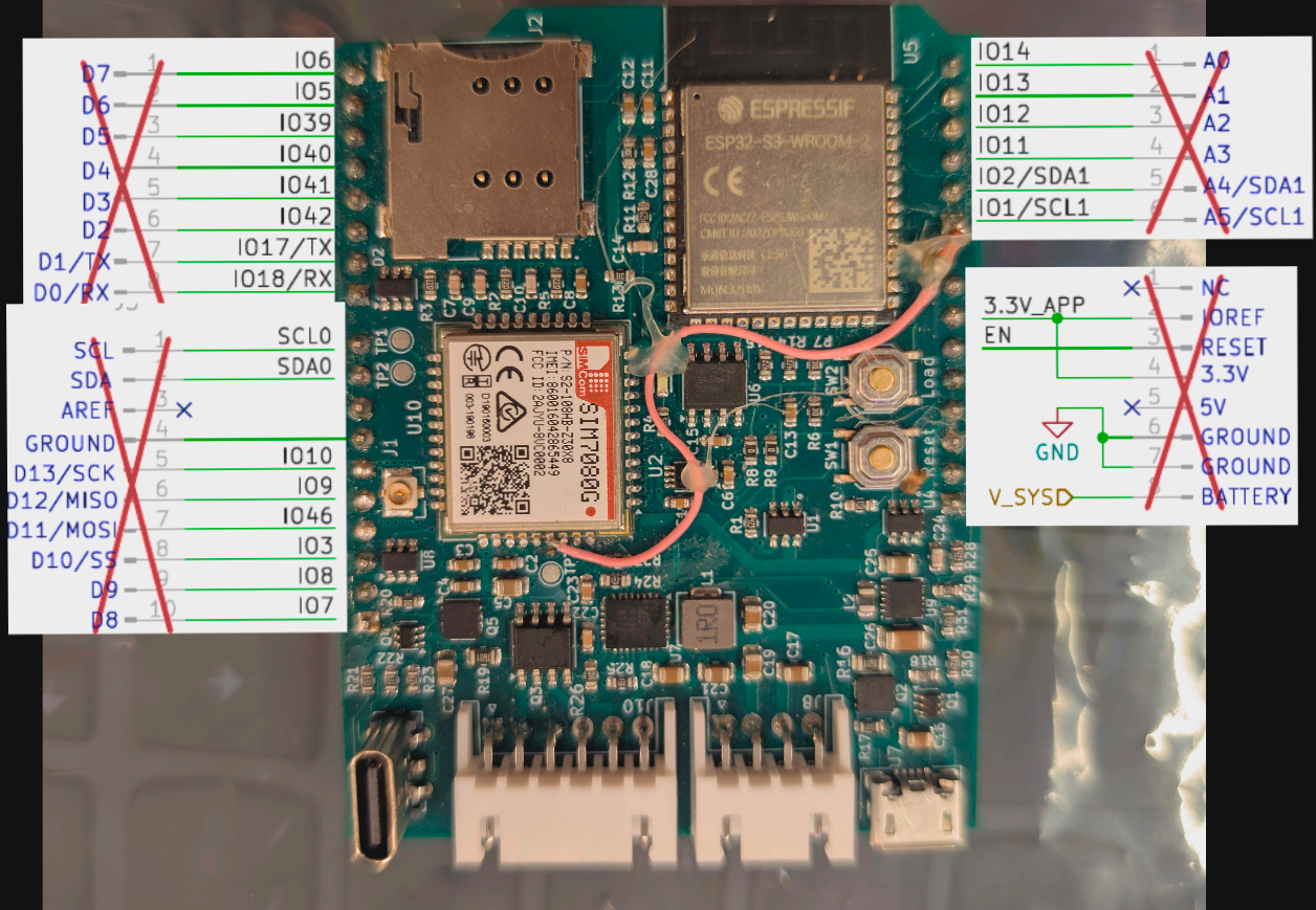
Global pinout
Issues
- The schematic has some mistakes, for example the PWRKEY pin of the SIM7080G is grounded directly instead of being connected to the MCU. Making it bootloop. There is a bypass wire on the board. We haven't been succesful in getting the SIM7080G to boot.
- We can't get pins of the MCU to work as expected. For instance we having issues getting pins to pull up. This could be due to incorrect board schematics.
- The board had trouble getting serial data. But to fix that we had to enable usb-cdc in the board config for it to send serial data